I came into possession of a Zeo XT long-term heart monitor (see image right). The device was sent to someone I know who ended up not using it. So I took it and, being curious, decided to crack it open and see what I could see.
The whole device was fascinating to explore and, without the benefit of knowing the designers, contemplate the design decisions.
Cracking it open
The is the cover. Note the blue dot. That’s a button I’ll show later on. [FYI, images follow explanatory text]
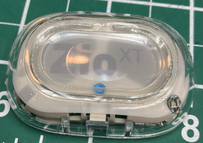
The cover opened up easily enough. Later, I realized it could be when the device is sent back, the technicians need to easily open it to access a micro USB port I’ll show shortly.
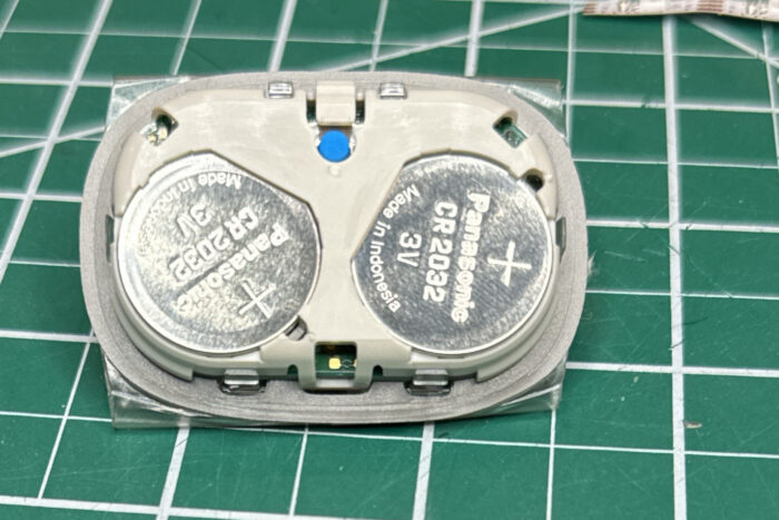
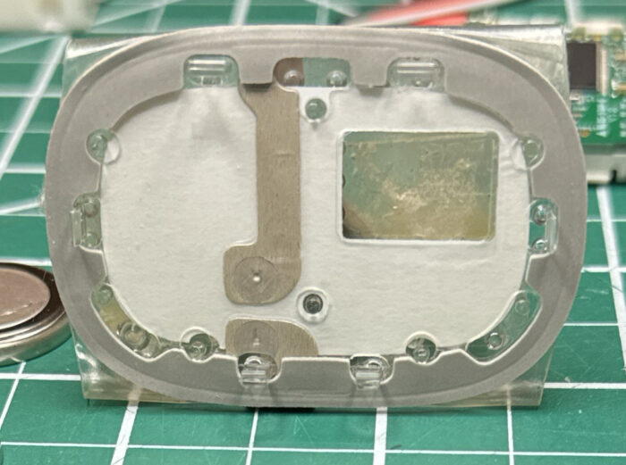
The bottom that the board sits on shows where the contacts for the leads come in, and you can see that there are divots for where the contact clips connect. There are also contact clips for the batteries. Smol. Smol.
That rectangle is the recess to accommodate the memory chip.
PCB
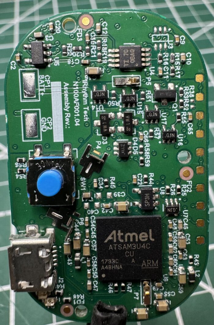
Lots of test points. View of both sides of the board. Closeups of some areas follow.
iRhythm Tech N100A6001.
Little clippy things for leads (in right image) and for batteries (in left image).
That big chip is the ISSI IS34ML04G08. NAND memory.
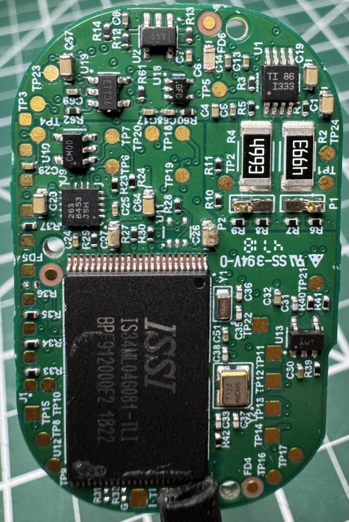
Closeups
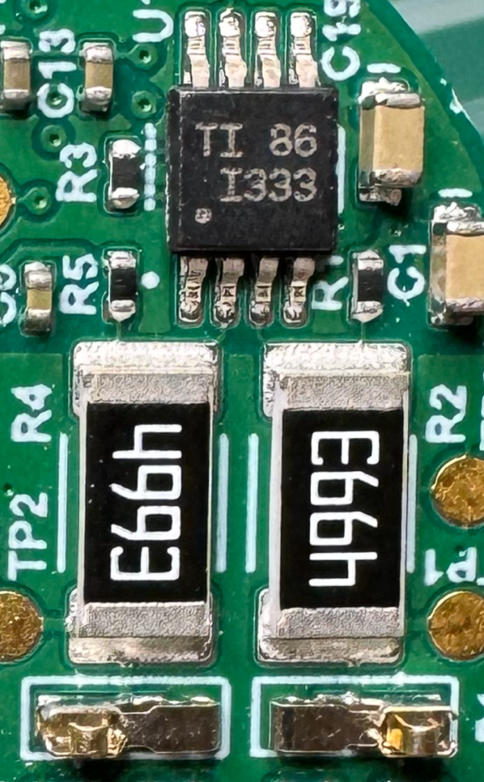
Right next to the clips for the leads (next to two large resistors) is a chip with TI 86 I333. This chips seems to be an INA to convert voltages into data.
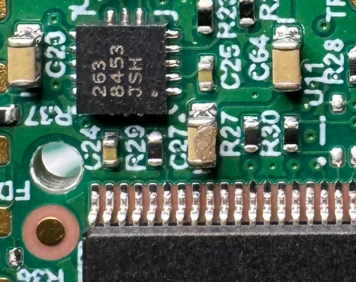
Next to the memory chip, this chip says 263 8453 JSH. I wonder if it’s a NXP MMA8543 accelerometer. Not sure why there’s an accelerometer on this. If that’s what that chip is. I was just Googling things, not chasing it too deep.
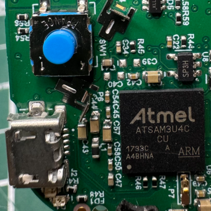
The MCU is a ATSAM3U4C
The architecture is designed to sustain high-speed data transfers. The multi-layer bus matrix, multiple SRAM banks, PDC, and DMA support parallel tasks and maximize data throughput.
Seems like data downloading is thru USB (which MCU supports). I think that’s why it’s so easy to disassemble.
And that’s a big blue button. The cover, shown earlier, flexes to click the button. This is the logging button that the user presses (when they feel an event?). Makes sense that it’s big and sturdy.
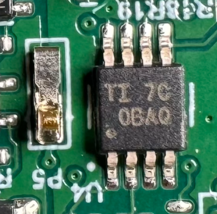
And here is an opamp.
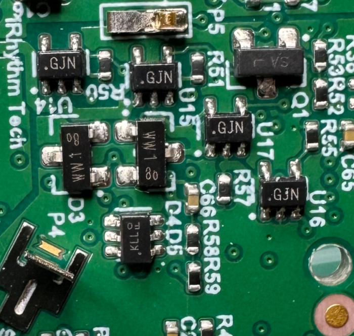
I think these are power regulators. And I think all this is to clean up power noise?
Also, you can see the clips nearby for the batteries at the top (negative) and bottom left (positive). Tiny tiny clips.
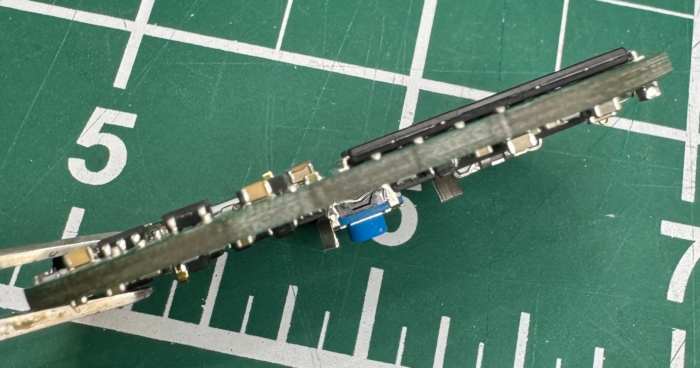
Layers, donkey
Lastly, I wonder how many layers the PCB is. It’s about 1.5mm thick. But that’s not a good measure for number layers I presume.
Yeah, I like investigating things like this.
