Mundane ‘aha!’ moments, mistakes, and mental models

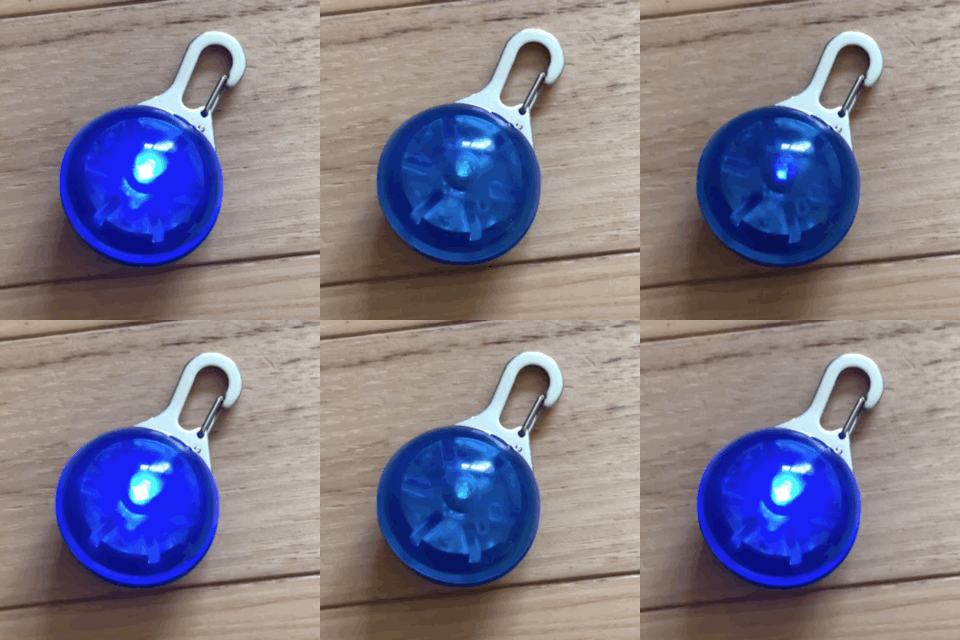
A while back, I bought some LED pendants that I put on my dogs when I send them our into the yard at night to do their business. The pendants help me see where they are and when they show up at the back door.

The pendants are really simple: an LED, a 5-pin IC (no markings), a cap and a resistor, and a CR2032 battery all on a simple PCB. Between the battery and the PCB there is some metal that makes a contact when you press the battery.

Being the dunce that I am, I was amazed that with one clicker the pendant could switch from fast blink to slow blink to steady light to off.

Ba-bam!
Then the other night it hit me. What the pendant was probably doing was doing a reset on a chip and the chip knew to cycle between the modes, going into deep sleep when LED was off.

Duh.
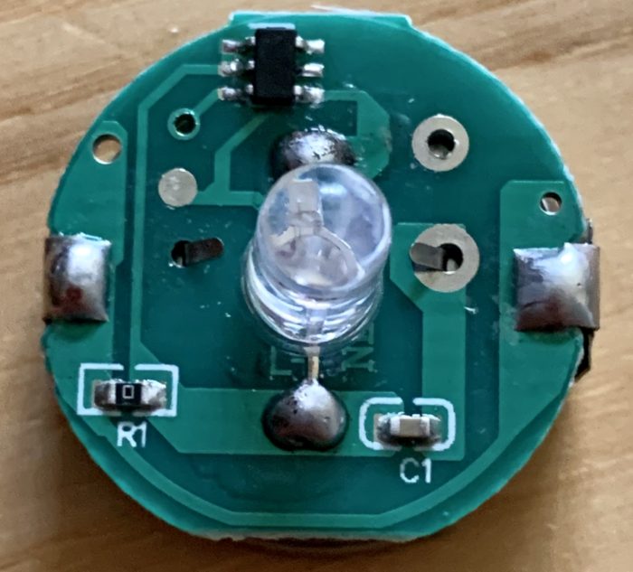
Not to be outdone, I wrote up a simple sketch that would do this, fired up my ATtiny programmer, and made my ATtiny45 (and 85) change modes of an LED every time I grounded the RESET, saving the state of the blinking in the EEPROM, going into sleep when the LED was off.

And just now, while writing this up, with this realization in mind, I broke open the pendant again and used my multimeter to find the VCC (pin 2), GND (pin 3), I/O (pin 4), and RST (pin 5) [pin numbering counter-clockwise from upper left in the, seemingly SOT23-5, IC in image to right]**. And with a jumper, I was able to ground the RST pin and cycle through the LED modes.

Mundane leveling up
Ok. I should have thought of this method the first time I opened up the pendant a few months ago and saw the metal clip that was acting as the button. For some reason I was stuck on ‘button’ and thought the cleverness was there.

But really, I don’t think I was ready to think the right way when I first opened the pendant. Something accreted in my mind in the intervening time that allowed me to know have this ‘aha!’ moment.

Also, I am proud of the skills I have gained* to quickly write it up and prove it out.

What I like of these little ‘aha!’ moments is that they push you into another plane of thinking, a new mental model, such that you now think differently from before the ‘aha.’

I suppose experience doesn’t give you the answer as to how to solve a problem, only more ways to think of how the problem can be solved. Before, I was limited, later on, I was not. And not only could I think of the process, but replicate it myself.

An aside on mistakes
I see a lot of newbies being afraid of mistakes. Though they relax when they learn from folks with much more skillz that mistakes happen to all.

For me, mistakes are a learning moment. The mistake teaches you the boundaries of the possible better than blindly following directions can. Through mistakes you can get more ‘aha’s than if you followed the instructions and did everything as you should. The ‘aha’s are important for the growth and expansion of your mental models.

And these mistakes can help you discover things you wouldn’t if you stayed on the path. History is crowded with mistakes that led to ‘aha’ that led to amazing things.

Lean into your mistakes. Better yet, try to make mistakes more regularly.

My wife, who loves to ski, always says, “If you’re not falling, you’re not trying hard enough.”

*It’s been one year since I set out to build my work demo that led to an exploration of electronics. I’m surprised by how much I learned in this time and what I’ve been able to do. Of course, looking forward to the second year.

**No markings means that I’ll have no way of finding what this chip is.

The Twelve Projects of Charlie

Based on my notes, on 15jul20 I will have completed one year since I started researching and designing a project for work that set me off on my crazy maker ride. Thinking of my next year of making, I’ve been pondering a challenge for myself. 

What I came up with is a challenge to do 12 different projects over the course of the year, one for each month. I thought of other frequencies, such as something daily or weekly, but monthly fits in well with what I can do and the nature of the projects I’ve been pondering for the challenge. Also, “12 projects” reminds me of the “12 labors of Hercules”. Haha.

Topic, style, theme
I really don’t have a general topic or style that would tie the 12 projects together other than they have to have a physical component (though not necessarily only chips and hardware). I am, though, challenging myself to have a common thread across all the project: I want to make things that have meaning. 

I love the ingenious and whimsical things I see others make. But, I want to do things that make folks think, or better, reveal things that were not visible before. I think this ties to my efforts at building ‘tangible experiences’, experiences that make the invisible manifest, to make physical representations of concepts.

Awakening a sense of fearsome wonder in the ordinary
When I say ‘meaning,’ I don’t mean beauty. There are plenty of artistic makers creating beautiful things with circuits and chips. I want to do more than beauty. I want to reach for the sublime.

I’ve done some reading over the past years about the sublime and the feelings one has when confronting the sublime. Historically, the sublime is attached to religious connotations, the feeling of awe and fear when encountering God. Indeed, I read an interesting article on 17th century religious fairs that had interactive displays to help folks connect to the sublime and feel the fear and awe of the sacred.

As a scientist, though, I have always been interested in the sublime in Nature, feeling awe and fear at the immensity of the cosmos, the interconnectedness of life, the processes of chemistry, and all sorts of changes that have happened in the past 13.5 billions years of reality.

Why the sublime? Already before the pandemic and the protests, I felt that at so many levels, not that we lost our way (that’s too cliche, and I can go on why that’s a lame cliche at that), but that we could use a reaffirmation of the meaning of being human, in the world, with other humans and organisms. Also, this interest in the sublime ties into my current philosophy of “wanting to spread the love I can give, do the good I can do, focus on me and mine, and grow from there.”

The past few weeks of protest, at the end of a few pandemical months, have really thrown me for a loop and suggest that now is a good time for such an exploration that this challenge affords. Connecting with the sublime, seeing that unseen that sits behind the curtain and in the interstices of our everyday reality could perhaps help us squabble lesss, find meaning in what we do, and become better beings.

Back to the projects
I do not think I’ll be able to connect the sublime with each project. Or the connection to the sublime might be forced. But attempting to connect to the sublime will be in the back of my mind as I choose and make these projects.

Interestingly, sometimes I have a hard time articulating in words something I inuit. Challenging myself to make things that help someone tangibly connect to the sublime and experience awe mighty be a way for me to articulate what I mean.

Let’s see.

image from GreekMythology.com

Working up to a proto step by step

I just posted a description of a tangible concept demo I recently built.

There were a few new things in this, such as learning how to use the serial connection, working with a optical isolator, that I did my usual step-by-step approach to it.

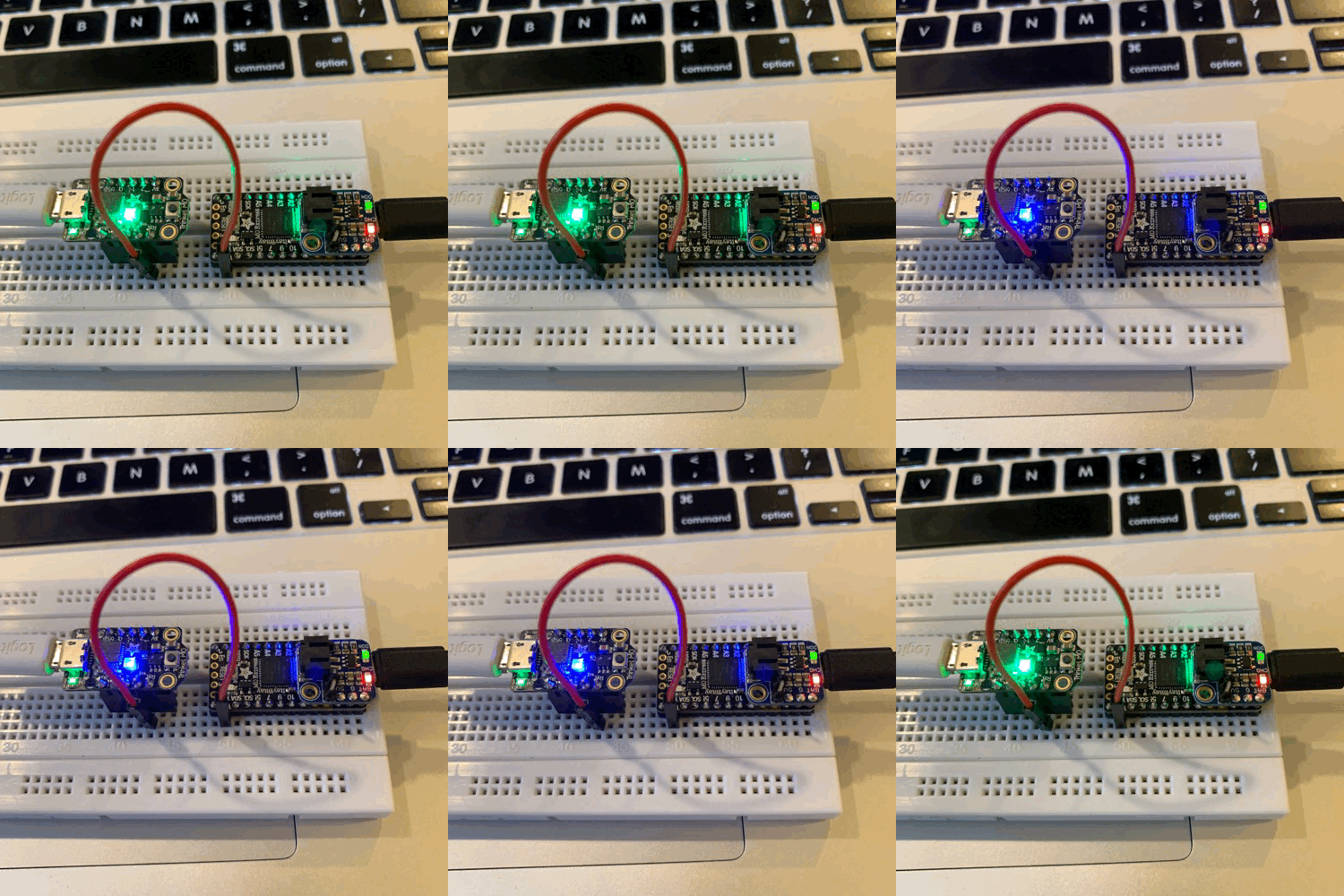
First, I needed to learn how to use serial communication between two microcontrollers. I used a Trinket and an ItsyBitsy I had lying around, connected them, and programmed them to send and receive data on the serial port using a version of the basic Arduino Serial example sketch. Good.

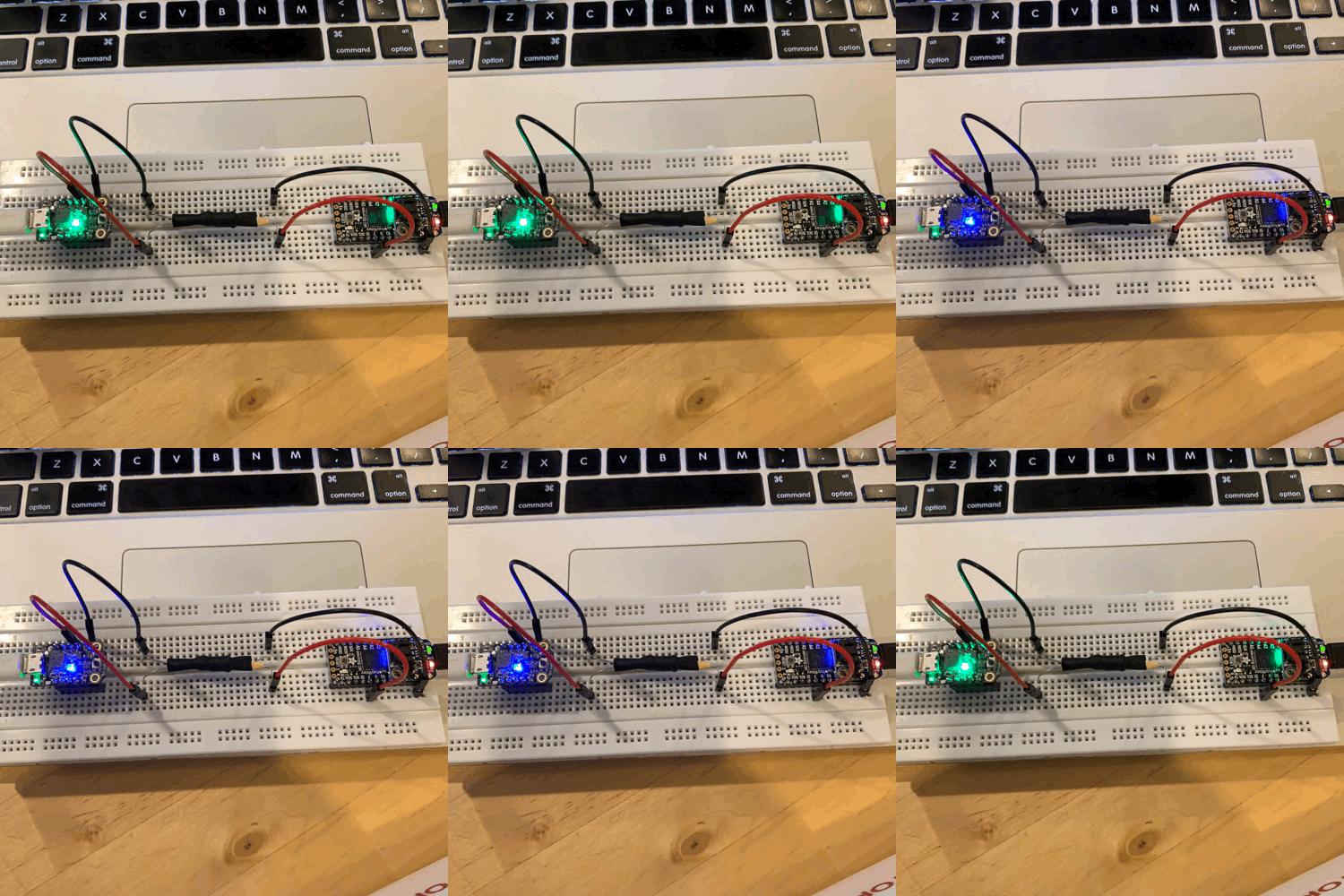
Then, as I didn’t have an optoisolator around, I made one from an LED and photoresistor I had lying around.

I then played around with the serial communication through that, learning about sensitivity, slowness, and the like. But it was enough to nudge me into researching optoisolators to get for the next steps.

Next step was to pass serial communication between the two boards, but via a proper optoisolator.

I’m not going to mention all the interesting errors I did trying to work this up, but suffice it to say, opoisolators are quite interesting chips (and thank good ness for data sheets and application guides from the manufacturer).

Once I understood how the optoisolator worked, I then programmed ATtiny84 microcontrollers to use the optoisolators and wired up a breadboard with jumpers to see if I could replicate things with the bare chips.

When I was satisfied with that, I started adding buttons and more LEDS and added more functionality to the code until I had something working. To clean things up, I then made used some cut-to-size wiring to make it easier to use the breadboard proto.

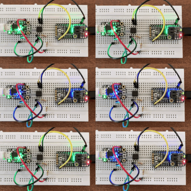
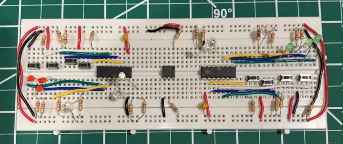
Here it is, mid-build (notice optoisolator at center not yet connected).

I did a write up here, with a video of the prototype in action.

Enjoy.

Where do I go from here?
I had worked up a proper schematic to help me built the proto. If I were to continue this, I’d make the schematic with a PCB in mind, lay it out, and then get some boards to actually build this – in a much smaller footprint.

Alas, I stopped the project at this stage. Perhaps I’ll get a nudge to pick this up later. 🙂

Optoisolation and tangible concept demonstration

I work at a company that offers hardware-based cybersecurity products and services. Our major product is a network appliance, called a data diode, that restricts data flow in one direction (meaning you can’t hack in the opposite direction).

Before you gasp in shock, it’s a real thing, needed by real people. For example, nuclear power plants use them to secure their operational networks (OT). The data diode allows them to stream their operational data out of the OT to their enterprise networks (IT) without allowing hackers to attack or send commands into the OT.

And it’s not just critical infrastructure folks who are interested, military and intelligence organizations use us to defend their networks and data.

So there.

Self-isolating
A core concept for our data diodes is the enforcement of one-way data flow using optical isolation – usually a light transmitter and receiver pair connected with a fiberoptic cable. That means the reverse direction can’t happen. And, without the optical connection, the two sides of the data diode are effectively ‘air-gapped’.

Optoisolator chips are similar: a light diode on one side, paired with a photoresistor on the other side. Optoisoloators are usually used to isolate networks with different voltages, allowing a signal to go from one side to the other without having to unify the two voltage nets. For example, say you have a 3.3V microcontroller and you want to drive a 120V speaker.

How it works
To make one-way transfer via an optoisolator more tangible, I built a prototype where two microcontrollers communicate via an optisolator. Buttons on either side are pressed and the button states are sent to the other side (via serial, if you must know), reflected in the indicator LEDs.

I chose the ATtiny84, as it is a nice and small microcontroller (MCU) and has more pins relative the more common ATtiny85. The optoisolator was the common 4N35. The rest is a bunch of wires (this being a breadboard proto), LEDs, resistors, and buttons.

For the data connection, let’s call the blue side the side that can transmit (TX) the state of the buttons through the optoisolator. The red side receives (RX) the button states. Clicking a button on the blue side will light up the corresponding LEDs on the blue and red side (the red side receiving the update). If I click a button on the red side, only the LED on the red side changes, as the red side can’t send data to the blue side, due to the optoisolator and also because the TX of the red side is not connected to the RX of the blue side.

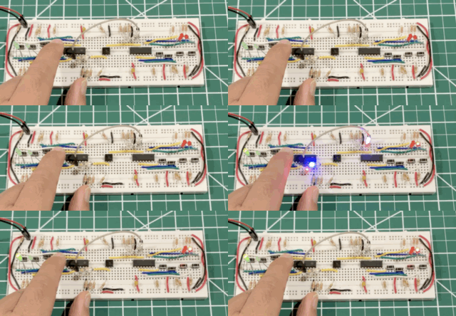
But I put the same code on both MCUs, so the red side MCU is still trying to transmit the button states. I can show this by bridging the optoisolator with a jumper wire connecting the RX of the red side and the TX of the blue side. With the jumper in place, a button press on the red side will show a corresponding change on the blue side.

Visualizing something simple
This is a way to show how you can have something that keeps data flowing in only one direction. And the jumper shows that you actually have to physically bridge the optoisolator to get transmission in the opposite direction.

Ideally, I wanted to make this into a badge folks could play with and hack. But perhaps later. Also, the way we build our data diodes, we actually have proxies on both sides of the gap to handle more complex communication on each side of the diode. I’ve been wondering of a way to make that concept more tangible, and I have an idea how that doesn’t use MCUs. But that, too, perhaps for another time.

Summary
This build is part of some exploration of mine to make some concepts more tangible. What drives me is to how to show things that can’t be seen, how to make the digital more physical.

Check out the video below for how the proto worked out and let me know how I did.

Building another tangible experience

At the end of last year, one of our product managers heard about my bioreactor demo. He thought it would be great to have something similar for software he was getting ready to launch for his product.

The software (used on our other data diodes) lets one set up Modbus registers to be read by the client on one side of the data diode and then set up the server on the other side of the diode to be read by a Modbus client.

Due to the holidays, we only were able to get together to talk about it mid-January, and then he told me he wanted something to show at an event at the end of February. So time was already getting tight, not to mention the time it took for him to get approval for the funds and the project.

In the end, I had about two weeks to design, build, test, and deliver something.

Catching the Modbus
The software was to provide Modbus compatibility for our DiOTa, the smallest of our data diodes. This was a big deal, as a lot of organizations were interested in using the DiOTa with Modbus across their critical infrastructure networks.

The hardware I was building was to provide a server and client to flank the diode. But principally, it was to be much more attractive, engaging, and interactive than the usual tablets and interfaces we have traditionally used to demonstrate our software and hardware.

I knew nothing about the technical underpinnings of Modbus when we started, but luckily there was an Arduino library. And, while I wanted an excuse to use new boards, we decided to reuse as much of my bioreactor set up as possible.

So, in about a week, I ordered what I needed, leveled up on Modbus, and built a fun set up for the product manager.

Mix of new and old
The library would not run on my Uno (the Uno barely had the memory for it), so I purchased two Adafruit Metro M4s. One would be the client and one would be the server. I went with the Metro as we had one Arduino Ethernet shield already and an I/O shield we could easily use to connect some of the sensors we had, so we stuck to the Arduino form factor (I so wanted to use a Feather).

I also wanted something with flash, so we decided to get an LED Matrix and Matrix Shield to show the data as it was read by the Modbus client stack (alas, the matrix shield needs so many pins, that we couldn’t put it on the server stack). On the server stack we added a battery shield, as we were initially planning to make the demo in a power distribution theme.

And, in a total impulse buy while perusing the shelves at Microcenter (always a bad thing), I picked up a dirt cheap light sensor (and smaller than a pinky fingernail!).

Keep in mind, the time constraint was a major driver in what we chose to use for the build.

We ended up with a temperature sensor, a magnet sensor (to simulate opening and closing of a coil), and a light sensor. We were also sending across to the client the uptime of the server and the battery voltage of the battery shield. Most of this changed dynamically – holding the temp sensor to raise temp, placing or removing a magnet from the magnet sensor, flashing light or covering the light sensor, and turning off or on the main power to go onto battery power.

Fun stuff.

And she said, and she said
I had it up and running in about a week (nights and weekends style, as building this was not part of my usual role at the company – the bioreactor was). I then headed down to the office to train folks on how to use it and see how well it worked with the data diode.

All went swimingly and we were all thrilled to see the sensor data updating at the client across the data diode.

Turns out that our head of training saw the demo setup and saw the value of the demo for training.

Then a few sales guys saw it and asked to use it for client demos.

This thing had legs!

Screeching halt, sort of
While the bioreactor was all for me, this was the first time I had to build something for someone else in the company. The build was also a test of the idea of using readily available maker hardware to help explain a concept. Basically, turning a technical demo into a more tangible experience, which I’d like to explore further.

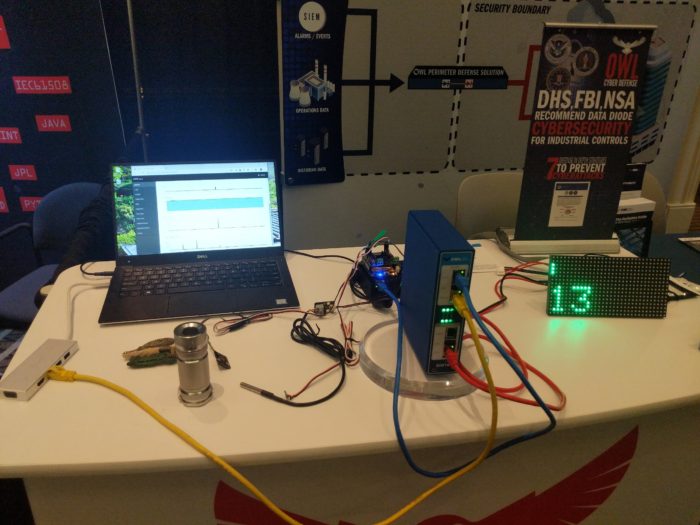
Alas, soon after the product manager returned from showing the set up at his event (photo above – good feedback, too) the whole world shut down and I have not been able to modify the demo or make extra ones (such as for training or sales) or explore other demos. All discussions of tangible experiences has sort of died down.

Oh well. The project was fast and fun. And I’m itching to get another commission.

In any case, I haven’t stopped exploring other ways to show concepts in tangible ways, like a physical narrative of the digital, or something like that.

And that’s a story for another post.

Learning to KiCad with the other foot

My wife, who was a crack soccer player in her youth and an overall able athlete, is full of sport metaphors for life. One, particularly relevant to the story today, was “Learn to kick with your other foot.” Basically, being able to kick well with both feet opens up so many more possibilities for you in a game.

Soaring to another tool
I’ve been taking an PCB skills class. When the class started, everyone had to mention what eCAD tool they were using. I’ve designed a few boards on Eagle, chosen as my first eCAD tool because there were many tutorials already. I had heard of KiCad, but an initial peek around it wasn’t too appealing.

For the PCB class, Eagle was a major tool used by the students. But I was intrigued how many also used KiCad. And, in the name of ‘kicking with the other foot’ decided to make an effort to learn and use KiCad for the course.

Getting to Hooked
In the PCB course forums, folks mentioned the Getting to Blinky tutorial series by Chris Gammel, from Contextual Electronics. The series is a few hours of going through all the key features of KiCad as you build a tiny blinky badge.

The series was very fun, perhaps too fun as I zipped off an order to Oshpark without critically thinking of any potential mods I’d like to do (which, of course, came up after I ordered the boards and components).

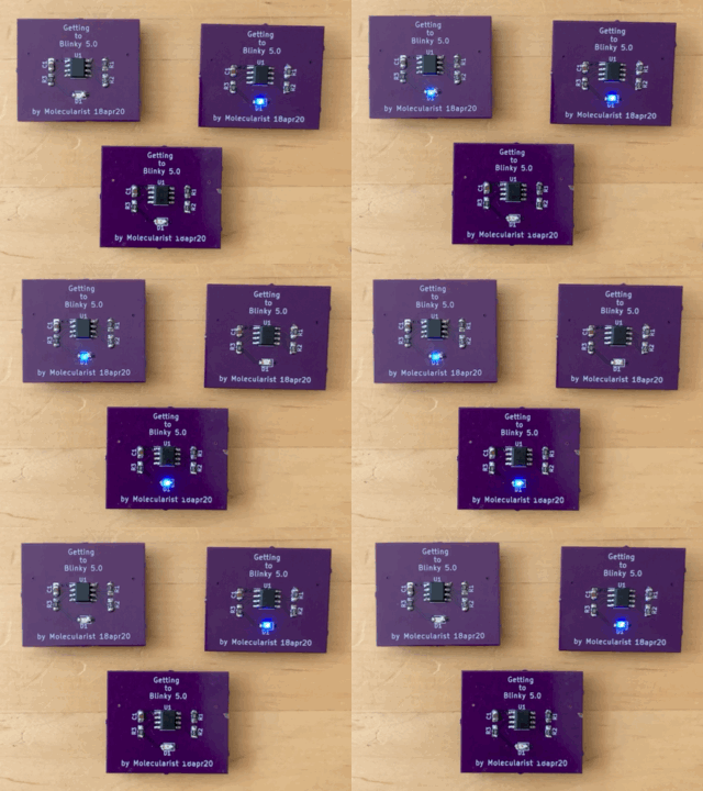
Nonetheless I was thrilled to get the boards and solder them all up (GIF above shows complete badges).

First time for everything
The other great thing about the tutorials is I ended up with a PCB that would need surface mount components. So, when I assembled the badge, I had my first experience with SMDs. Nowhere near as impossible as I thought.

Which comes to the heart of the subversion of the series: you can do it – you can design a board, order parts and PCBs, and solder the SMDs.

And that’s a great feeling when you realize that.

Hacking hardware

This past month or so I’ve delved into hacking hardware (not building, but taking apart). I’m leading the efforts at Owl, the company I work with, to expand their device inspection and analysis service to medical devices. As part of this work, I have been learning quite a bit about how hardware can be inspected and hacked.

Grand ideas
I had no intention to go deep into hardware snooping, but, while reading up on DEFCON #badgelife, I stumbled upon Joe Grand, also known as Kingpin of the notorious L0pht Heavy Industries of the 90s. I had heard of L0pht back in the day, so it was quite interesting to catch up with what Joe and his cohorts have been up to since.

While Joe is one of the fathers of #badgelife, I started reading up on his hardware hacking. Quite fascinating topic.

Crossing streams
Then, while doing apparently unrelated research on optoisolators and hacking data diodes for a demo I am building, I stumbled upon a video showing how to create an out of band connection over a data diode via RF.

You now how this goes. Digging deeper into the guy mentioned in the video, Monta Elkins, I found his SANS instructor’s page and a presentation his did on jumping air gaps.* More searching and I came upon this incredibly interesting and fun presentation of hacking 20 things in 45 minutes (getting root access to a bunch of consumer electronics). Then I watched Monta’s DEFCON presentation where he uses an electric drill as a proxy for hacking an industrial logic control.

Drilling into the subject
The video did a great job reinforcing all the things I had been learning from our own hardware guys, reading about Joe Grand and others, and other research into hardware inspection and circumvention (always about circumvention – we are in the cyber security space, after all).

Two things I want to point out from what Monta said in the electric drill presentation.

First, he was examining the firmware and showed how knowing the hash of the code of the firmware, one could check for a compromise. So, Monta asks, should manufacturers publicly publish hashes of their firmware so we could verify the software is good?

Secondly, with all this hacking, he pointed out that things would have been easier if the programming pins were on the outside. So, he ask, should manufacturers make their programming pins accessible from outside their device to make it easy to check firmware, make mods, and the like?

Both are interesting questions.

Not just academic
OK, so I mentioned at the top I had not intended to get deep into hardware hacking. But it fit well the path I’ve been taking. At first, I wanted to turn to our own device inspection experts to help me get the word out on Owl’s device inspection services. But after talking to our experts, reading and researching the topic, and validating my thoughts with our experts again (I don’t want to say something impossible), I did a hardware inspection of my own.

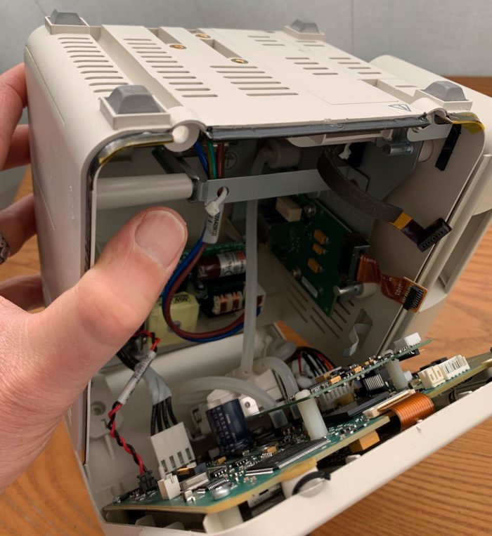
I had purchased a patient monitor for our experts to examine, but the shutdown (and their schedules) got in the way. So I did it myself. And did a webinar on it. The webinar is a great summary of all that I learned on this hardware hacking journey (and you get to peek inside a patient monitor).

Fascinating. And looking forward to doing more.

*In case you’re interested, here are two more examples of jumping air gaps, via RF and via power supply vibration.

Pause for station identification

Wow. The world is such a different place since my last station identification. I’m writing this in the midst of the largest global disruption since perhaps WWII. Though, since last station ID I’ve also learned and grew in ways I had no inkling I was able to 5 months ago.

Me
Who am I? I’m Charlie Schick. I’m passionate about exploring how the intersection of bits and atoms help us form the narratives of our physical-digital-sublime world; particularly how we use physical constructs to connect to the sublime. I also advise companies on product design and strategy, market insights, and innovation strategy. I’m a recovering PhD, too, and proudly ex-IBM, -Boston Children’s, -Nokia.

Right now
My current 100% is with Owl Cyber Defense, a cybersecurity hardware and service firm. I lead their business development and corporate innovation in healthcare and the life sciences, growing a new segment for Owl products and services by uncovering and establishing new and innovative business, partnering, and product opportunities.

I see myself occupied by Owl for the foreseeable future, though outside of Owl, there have been some other fun developments.

One more thing: I enjoy sharing my experience, insights, and exploits, especially through writing for and speaking to large audiences and engaging with others in stimulating conversations, including the office of CxOs. Let me know how I can help in this capacity.

And of course, my standard disclaimer
(my usual riff off of an ancient Cringely disclaimer)
Everything I write here on this site is an expression of my own opinions, NOT of any of my clients or anyone I work for, especially Owl. If these were the opinions of my clients or Owl, the site would be under their name and, for sure, the writing and design would be much more professional. Likewise, I am an intensely trained professional writer :-P, so don’t expect to find any confidential secret corporate mumbo-jumbo being revealed here.

If you have ideas or projects that you think I might be interested in, please contact me, Charlie Schick, at firstname.lastname@molecularist.com or via my profile on LinkedIn.

Yes, you can find me on Twitter. But after many times paused with my finger on the ‘delete account’ button, and letting all my social media channels go fallow, I’m really out of practice, so perhaps now’s not the best time to message me there. Feel free to try, though. Might be good for my Twitter ‘rehab’ (that doesn’t read right, does it?).

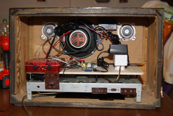
Image from The-radio (a radio converted to use a Raspberry Pi)

The value of the open source community

One of the most valuable components of open source hardware and software making is availability of code and guides built by a community around a solution, hardware, or topic.

The corollary to that is that no open source solution or hardware will succeed without a critical mass of active users.

Duh
Ok, so that might sound obvious. But let me illustrate what happened to me last week.

I’ve been breaking down and inspecting a patient monitor recently. I wanted to have it send some HL7 messages to a server, so I could see the kinds of messages and see how that messaging can be hacked. I had a Raspberry Pi 4 from another project looking for something to do, so I typed in ‘open emr raspberry pi’ to see what I could find.

There were a few. Cool. And there was one that already had an image for the Raspberry Pi. So I downloaded it, put it on a SD, and then tried to use it.

Nope. It was only for the Raspberry Pi 3.

No worry, there seemed to be a wiki with instruction on how to install it from scratch. Though it seemed like there were some missing pieces, the code was a bit too generic for Raspbian, the applications to download didn’t really map to PyPi where it as coming from.

No worries. I slowly worked my way through things, stepping forward, and falling back as I did my troubleshooting. What became obvious was that not many folks seemed to be talking about the process, so I really was flying blind, no examples, tips, forums, guides to help me in the install.

Ok, worries. I saw what hinted to be easier ways to install from PyPi. Why wasn’t that in the official guide? Why didn’t the PyPi stuff match the stuff in the official guide?

No matter. I managed to get the EMR server up and running, learning along the way what was needed to make this thing run.

Then I tried to install the client. And the official guide wasn’t helpful at all for a n00b like me to sort out the errors. Why was it so f-in hard to just install the damed thing? Hadn’t this EMR been around for years?

I then saw that what little was written up for this EMR talked about SUSE, a distribution of Linux I didn’t know at all. But the SUSE site had a guide for installing this EMR. So I loaded SUSE on an SD and did the painful thing of setting it up to use.

Though this time I set a time limit, as the whole process really was disheartening.

Needless to say, the time ran out.

Community helps
That evening, looking back on the two or so days I was trying to make this happen, I realized the value of a broad user base sharing code and insights.

I’ve built a ton of projects, designed boards, coded things – all with a backdrop of guide, tutorials, example code, easy to deploy tool chains, and lots and lots of community chatter.

I couldn’t find anything of the sort for this EMR (and I think it’s been around for 10 years!). And the lame state of the official guide, websites, and such suggests that this isn’t really something that I can do.

Two lessons
The first lesson is for me – stick to things that reside in a healthy ecosystem of code, hardware, examples, history, and people to talk to.

The second lesson is for all of us – if you want to succeed, make an effort in building that ecosystem, one the feeds on itself and rapidly grows as folks use what you make, share what you make, and hack what you make.

A belated realization
When I was selling a Hadoop version way back when, I was wondering why the more established players flaunted the levels of commits and the like.* I knew it was a proxy for interest. But now I know that it’s also a proxy for examples, creations, and support from the community. That should be considered also when choosing software or hardware platforms to build upon.

Right?

What do you think? Do you have similar stories?

*Actually, when reading up on a repo on GitHub, I always look at the last commit dates, not only to see how active the repo is, but to tell me if I’m going to have any trouble. This isn’t a petty thing to think of, but actually an important indication of things such as quality, relevance, and usability (as I guess I’ve always implicitly known, reinforced by this EMR fiasco).

Image by Tumiso

Fun with cardboard circuits

The usual progression for making printed circuits is (very roughly) you design the circuit, prototype it on a breadboard, design your PCB, and iterate on your PCB design.

Impatient hands
I’m a bit too impatient to wait for the PCB part. Also, I learn better having things in my hands. Iterating at the PCB design level, where you need to wait days, if not weeks, for your PCB board to come back, isn’t ideal for my impatient ways.

What I noticed is that after prototyping the circuit, I like to lay it out on cardboard. Doing this gives me a feel for scale, arrangement, and process.

Of course, for now, I’m doing it with through-hole components, though I am debating doing it with with surface mount devices.

One thing at a time.

As for ‘one thing at a time‘, cardboard prototyping also fits in well with how I set myself to learn. I get to focus on one thing at a time. Be it, design, or new arrangement of parts, or a new circuit type. I think before you hit the PCB design, the level of learning to get there needs a few more steps than usual.

Some recent cardboard projects
I mentioned what I’ve been doing to learn #badgelife concepts. The whole process of printing and pasting onto cardboard was helpful in giving me an understanding of scale and packing of components.

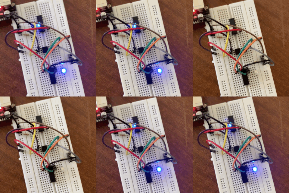
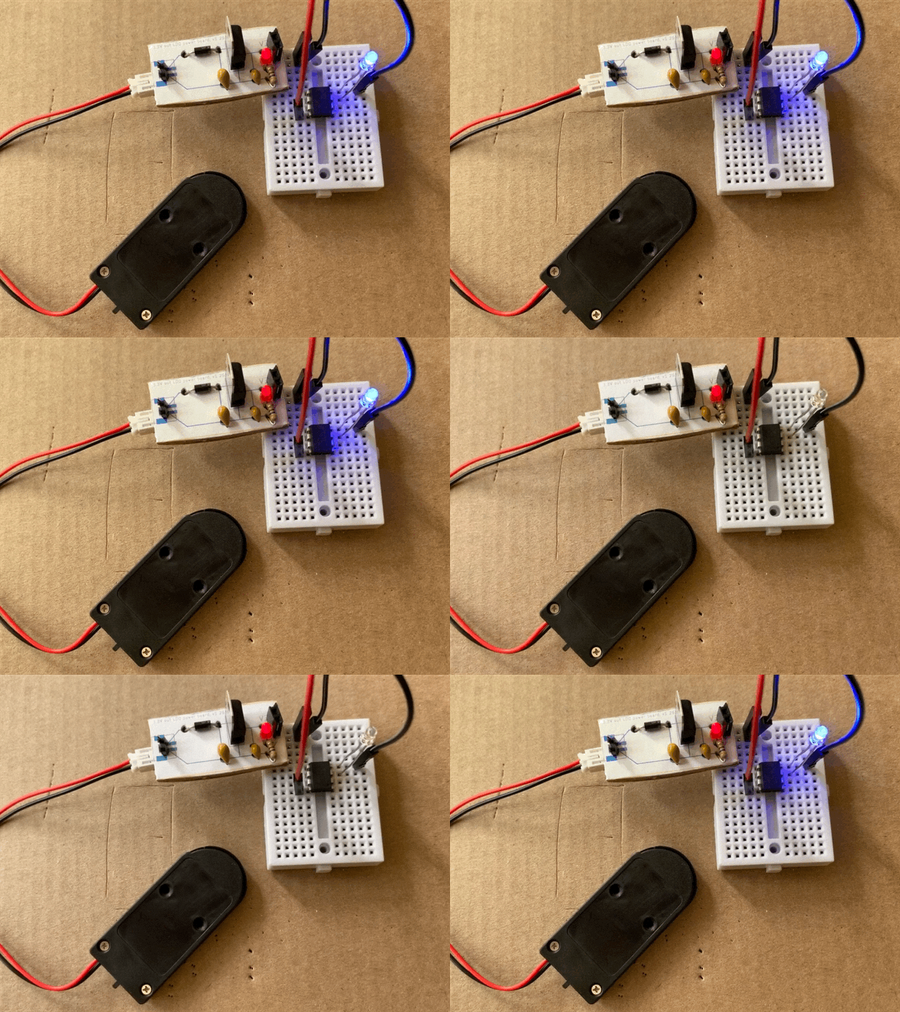
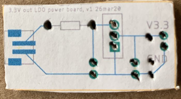
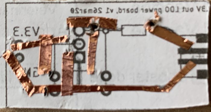
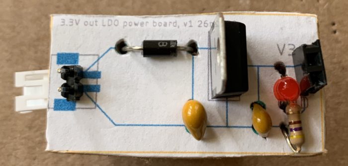
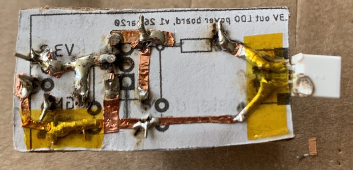
Yesterday, I spent the day building a 3.3V power regulator on cardboard (see GIF above of it in action). I had read schematics on how to make one. Bought components to try it out on a breadboard. And then put it on a schematic to print and guide building of the circuit on a piece of cardboard.

Interestingly, by futzing with it in my hand, I saw an opportunity for an on-the-fly change, adding a resistor and a diode to indicate power was on.

And the process reinforced some insights I gained while doing other similar cardboard-based circuits around soldering on the copper tape, handling and laying down copper tape, bridging the components and the coper circuit, and, of course, scale.

Surface mount, anyone?
From the cardboard proto of that owl badge I’ve been working on, I went and made a PCB. The PCB will be for through-hole components. The exercise was really to see if I could make a custom outline, silk, resist, and copper pours (fun stuff). I didn’t want to also have to learn other SMD-related issues.

Also, I know when the board comes in I’ll learn a bit about handling the boards, soldering many boards, and how might it hang from a lanyard – things I knew best learned with a first run of PCBs.

The next step is to convert the badge to mostly SMD, mostly to keep the front pristine, but also to learn how to search and buy surface mount components (soooo many). But I’m wondering if I should do a round of cardboard protos, first. SMD components will allow me to shrink the board somewhat (sand save money). Might want to try that out on cardboard rather than via PCB iterations.

Let’s see. In any case, I will report back.

And then there’s brass
As a parting thought, I read up on free-form circuits built from brass rods. Check out these guys. Lovely sculptures.

Haha. One more process to learn and tinker with.

What about you?
What materials are you working with outside the usual? Wood? Paper? Fabric?

Let me know Send me links of your work!